- 您现在的位置:买卖IC网 > Sheet目录1903 > AT89C51ID2-RLRIM (Atmel)IC MCU FLASH 8051 64K 5V 44-VQFP
84
AT89C51ID2
4289C–8051–11/05
When the slave address and the direction bit have been transmitted and an acknowl-
edgement bit has been received, the serial interrupt flag is set again and a number of
status code in SSCS are possible. There are 40h, 48h or 38h for the master mode and
also 68h, 78h or B0h if the slave mode was enabled (AA=logic 1). The appropriate
action to be taken for each of these status code is detailed in Table . This scheme is
repeated until a STOP condition is transmitted.
SSIE, CR2, CR1 and CR0 are not affected by the serial transfer and are referred to
Table 7 to Table 11. After a repeated START condition (state 10h) the TWI module may
switch to the master transmitter mode by loading SSDAT with SLA+W.
Slave Receiver Mode
In the slave receiver mode, a number of data bytes are received from a master transmit-
ter (Figure 34). To initiate the slave receiver mode, SSADR and SSCON must be loaded
as follows:
The upper 7 bits are the address to which the TWI module will respond when addressed
by a master. If the LSB (GC) is set the TWI module will respond to the general call
address (00h); otherwise it ignores the general call address.
CR0, CR1 and CR2 have no effect in the slave mode. SSIE must be set to enable the
TWI. The AA bit must be set to enable the own slave address or the general call address
acknowledgement. STA, STO and SI must be cleared.
When SSADR and SSCON have been initialised, the TWI module waits until it is
addressed by its own slave address followed by the data direction bit which must be at
logic 0 (W) for the TWI to operate in the slave receiver mode. After its own slave
address and the W bit have been received, the serial interrupt flag is set and a valid sta-
tus code can be read from SSCS. This status code is used to vector to an interrupt
service routine.The appropriate action to be taken for each of these status code is
detailed in Table . The slave receiver mode may also be entered if arbitration is lost
while TWI is in the master mode (states 68h and 78h).
If the AA bit is reset during a transfer, TWI module will return a not acknowledge (logic 1)
to SDA after the next received data byte. While AA is reset, the TWI module does not
respond to its own slave address. However, the 2-wire bus is still monitored and
address recognition may be resume at any time by setting AA. This means that the AA
bit may be used to temporarily isolate the module from the 2-wire bus.
Slave Transmitter Mode
In the slave transmitter mode, a number of data bytes are transmitted to a master
receiver (Figure 35). Data transfer is initialized as in the slave receiver mode. When
SSADR and SSCON have been initialized, the TWI module waits until it is addressed by
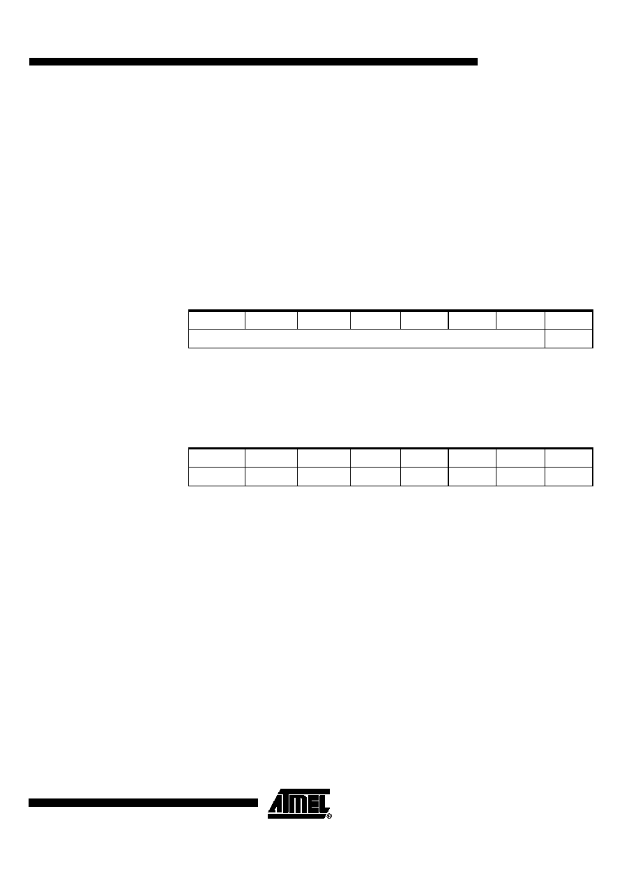
Table 63. SSADR: Slave Receiver Mode Initialization
A6
A5
A4
A3
A2
A1
A0
GC
own slave address
Table 64. SSCON: Slave Receiver Mode Initialization
CR2
SSIE
STA
STO
SI
AA
CR1
CR0
bit rate
1
0
1
bit rate
发布紧急采购,3分钟左右您将得到回复。
相关PDF资料
AT89C51RC-24PU
IC MCU 32K FLASH 24MHZ 40-DIP
AT89C51RC2-RLRIL
IC MCU FLASH 8051 32K 3V 44-VQFP
AT89C51RE2-SLRUM
MCU 8051 128K FLASH 44-PLCC
AT89C51SND1C-7HTUL
IC MCU 64KB FLASH MEM 81-CBGA
AT89C51SND2C-7FTUL
IC 8051 MCU FLASH 64K MP3 100BGA
AT89C52-24PI
IC MICRO CTRL 24MHZ 40DIP
AT89C55WD-24AU
IC 8051 MCU FLASH 20K 44TQFP
AT89EB5114-TGSIL
IC 8051 MCU FLASH 4K 20SOIC
相关代理商/技术参数
AT89C51ID2-RLRUM
功能描述:8位微控制器 -MCU C51ID2 64K FLASH 32KHz 3-5.5V RoHS:否 制造商:Silicon Labs 核心:8051 处理器系列:C8051F39x 数据总线宽度:8 bit 最大时钟频率:50 MHz 程序存储器大小:16 KB 数据 RAM 大小:1 KB 片上 ADC:Yes 工作电源电压:1.8 V to 3.6 V 工作温度范围:- 40 C to + 105 C 封装 / 箱体:QFN-20 安装风格:SMD/SMT
AT89C51ID2-RLTIM
功能描述:IC 8051 MCU FLASH 64K 44VQFP RoHS:否 类别:集成电路 (IC) >> 嵌入式 - 微控制器, 系列:89C 标准包装:9 系列:87C 核心处理器:8051 芯体尺寸:8-位 速度:40/20MHz 连通性:UART/USART 外围设备:POR,WDT 输入/输出数:32 程序存储器容量:32KB(32K x 8) 程序存储器类型:OTP EEPROM 大小:- RAM 容量:256 x 8 电压 - 电源 (Vcc/Vdd):4.5 V ~ 5.5 V 数据转换器:- 振荡器型:内部 工作温度:0°C ~ 70°C 封装/外壳:40-DIP(0.600",15.24mm) 包装:管件
AT89C51ID2-RLTUM
功能描述:8位微控制器 -MCU C51ID2 64K FLASH 32KHz 3-5.5V RoHS:否 制造商:Silicon Labs 核心:8051 处理器系列:C8051F39x 数据总线宽度:8 bit 最大时钟频率:50 MHz 程序存储器大小:16 KB 数据 RAM 大小:1 KB 片上 ADC:Yes 工作电源电压:1.8 V to 3.6 V 工作温度范围:- 40 C to + 105 C 封装 / 箱体:QFN-20 安装风格:SMD/SMT
AT89C51ID2-SLRIM
功能描述:IC MCU FLASH 8051 64K 5V 44-PLCC RoHS:否 类别:集成电路 (IC) >> 嵌入式 - 微控制器, 系列:89C 标准包装:1,500 系列:AVR® ATtiny 核心处理器:AVR 芯体尺寸:8-位 速度:16MHz 连通性:I²C,LIN,SPI,UART/USART,USI 外围设备:欠压检测/复位,POR,PWM,温度传感器,WDT 输入/输出数:16 程序存储器容量:8KB(4K x 16) 程序存储器类型:闪存 EEPROM 大小:512 x 8 RAM 容量:512 x 8 电压 - 电源 (Vcc/Vdd):2.7 V ~ 5.5 V 数据转换器:A/D 11x10b 振荡器型:内部 工作温度:-40°C ~ 125°C 封装/外壳:20-SOIC(0.295",7.50mm 宽) 包装:带卷 (TR)
AT89C51ID2-SLRUM
功能描述:8位微控制器 -MCU C51ID2 64K FLASH TWI 32KHz 5V RoHS:否 制造商:Silicon Labs 核心:8051 处理器系列:C8051F39x 数据总线宽度:8 bit 最大时钟频率:50 MHz 程序存储器大小:16 KB 数据 RAM 大小:1 KB 片上 ADC:Yes 工作电源电压:1.8 V to 3.6 V 工作温度范围:- 40 C to + 105 C 封装 / 箱体:QFN-20 安装风格:SMD/SMT
AT89C51ID2-SLSIM
制造商:ATMEL 制造商全称:ATMEL Corporation 功能描述:8-bit Flash Microcontroller
AT89C51ID2-SLSUM
功能描述:8位微控制器 -MCU 64K FLASH 32KHz 3.5-5V Ind. RoHS:否 制造商:Silicon Labs 核心:8051 处理器系列:C8051F39x 数据总线宽度:8 bit 最大时钟频率:50 MHz 程序存储器大小:16 KB 数据 RAM 大小:1 KB 片上 ADC:Yes 工作电源电压:1.8 V to 3.6 V 工作温度范围:- 40 C to + 105 C 封装 / 箱体:QFN-20 安装风格:SMD/SMT
AT89C51ID2-SMSIM
制造商:ATMEL 制造商全称:ATMEL Corporation 功能描述:8-bit Flash Microcontroller